

How To Draw Energy Band Diagram


In solid-land physics of semiconductors, a band diagram is a diagram plotting various primal electron energy levels (Fermi level and nearby energy band edges) every bit a function of some spatial dimension, which is often denoted x.[1] These diagrams help to explain the operation of many kinds of semiconductor devices and to visualize how bands change with position (ring angle). The bands may be coloured to distinguish level filling.
A band diagram should not be confused with a band structure plot. In both a ring diagram and a ring construction plot, the vertical axis corresponds to the energy of an electron. The difference is that in a band structure plot the horizontal centrality represents the wave vector of an electron in an infinitely big, homogeneous material (a crystal or vacuum), whereas in a band diagram the horizontal axis represents position in space, normally passing through multiple materials.
Because a band diagram shows the changes in the band structure from place to place, the resolution of a band diagram is limited by the Heisenberg uncertainty principle: the band structure relies on momentum, which is only precisely divers for big length scales. For this reason, the band diagram can only accurately depict development of band structures over long length scales, and has difficulty in showing the microscopic picture of sharp, diminutive calibration interfaces between different materials (or between a textile and vacuum). Typically, an interface must exist depicted equally a "black box", though its long-distance effects tin be shown in the ring diagram equally asymptotic band angle.[2]
Anatomy [edit]
The vertical axis of the ring diagram represents the free energy of an electron, which includes both kinetic and potential energy. The horizontal axis represents position, often not being drawn to scale. Note that the Heisenberg uncertainty principle prevents the band diagram from being drawn with a high positional resolution, since the band diagram shows energy bands (equally resulting from a momentum-dependent band structure).
While a basic band diagram simply shows electron energy levels, oftentimes a band diagram will be busy with further features. Information technology is common to run into cartoon depictions of the motion in free energy and position of an electron (or electron hole) as it drifts, is excited by a calorie-free source, or relaxes from an excited state. The band diagram may be shown connected to a circuit diagram showing how bias voltages are applied, how charges flow, etc. The bands may exist colored to betoken filling of free energy levels, or sometimes the ring gaps volition exist colored instead.
Energy levels [edit]
Depending on the material and the degree of detail desired, a variety of free energy levels volition be plotted against position:
- E F or μ: Although it is not a ring quantity, the Fermi level (total chemical potential of electrons) is a crucial level in the band diagram. The Fermi level is set by the device'southward electrodes. For a device at equilibrium, the Fermi level is a constant and thus volition exist shown in the ring diagram as a apartment line. Out of equilibrium (e.chiliad., when voltage differences are applied), the Fermi level volition non be flat. Furthermore, in semiconductors out of equilibrium it may be necessary to indicate multiple quasi-Fermi levels for unlike energy bands, whereas in an out-of-equilibrium insulator or vacuum it may not be possible to give a quasi-equilibrium description, and no Fermi level tin can exist defined.
- Due east C: The conduction band edge should be indicated in situations where electrons might be transported at the bottom of the conduction band, such as in an due north-type semiconductor. The conduction band border may too be indicated in an insulator, simply to demonstrate ring bending effects.
- E V: The valence band edge besides should be indicated in situations where electrons (or holes) are transported through the top of the valence ring such as in a p-type semiconductor.
- E i: The intrinsic Fermi level may exist included in a semiconductor, to show where the Fermi level would have to be for the fabric to exist neutrally doped (i.e., an equal number of mobile electrons and holes).
- Eastward imp: Impurity energy level. Many defects and dopants add together states within the band gap of a semiconductor or insulator. It can exist useful to plot their energy level to encounter whether they are ionized or not.[iii]
- E vac: In a vacuum, the vacuum level shows the free energy , where is the electrostatic potential. The vacuum can be considered every bit a sort of insulator, with East vac playing the part of the conduction band edge. At a vacuum-textile interface, the vacuum energy level is fixed by the sum of work role and Fermi level of the textile.
- Electron analogousness level: Occasionally, a "vacuum level" is plotted even inside materials, at a fixed height to a higher place the conduction band, determined past the electron affinity. This "vacuum level" does not represent to any bodily energy band and is poorly defined (electron affinity strictly speaking is a surface, non bulk, holding); notwithstanding, information technology may exist a helpful guide in the employ of approximations such as Anderson's rule or the Schottky–Mott dominion.


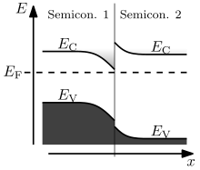
Ring bending [edit]
When looking at a band diagram, the electron energy states (bands) in a textile can bend up or down near a junction. This event is known every bit band bending. It does non correspond to any concrete (spatial) angle. Rather, band bending refers to the local changes in electronic structure, in the free energy offset of a semiconductor's band structure near a junction, due to space charge effects.
The primary principle underlying band bending inside a semiconductor is infinite accuse: a local imbalance in charge neutrality. Poisson's equation gives a curvature to the bands wherever at that place is an imbalance in accuse neutrality. The reason for the charge imbalance is that, although a homogeneous cloth is charge neutral everywhere (since it must be charge neutral on boilerplate), at that place is no such requirement for interfaces. Practically all types of interface develop a charge imbalance, though for different reasons:
- At the junction of two different types of the same semiconductor (due east.g., p-n junction) the bands vary continuously since the dopants are sparsely distributed and but perturb the organisation.
- At the junction of two different semiconductors there is a abrupt shift in band energies from 1 cloth to the other; the band alignment at the junction (e.thou., the difference in conduction ring energies) is fixed.
- At the junction of a semiconductor and metallic, the bands of the semiconductor are pinned to the metallic's Fermi level.
- At the junction of a conductor and vacuum, the vacuum level (from vacuum electrostatic potential) is set by the material'south work part and Fermi level. This besides (usually) applies for the junction of a conductor to an insulator.
Knowing how bands volition bend when ii unlike types of materials are brought in contact is cardinal to understanding whether the junction will be rectifying (Schottky) or ohmic. The caste of band bending depends on the relative Fermi levels and carrier concentrations of the materials forming the junction. In an n-blazon semiconductor the ring bends upwards, while in p-type the band bends downward. Note that band angle is due neither to magnetic field nor temperature gradient. Rather, information technology only arises in conjunction with the force of the electric field.[ citation needed ]
Run into also [edit]
- Anderson's rule – judge rule for ring alignment of heterojunctions based on vacuum electron affinity
- Schottky–Mott rule – judge rule for ring alignment of metallic–semiconductor junctions based on vacuum electron affinity and work function
- Field upshot (semiconductor) – band angle induced past an electric field at the vacuum (or insulator) surface of a semiconductor
- Thomas–Fermi screening – rudimentary theory of the band bending that occurs effectually a charged defect
- Breakthrough capacitance – special case of ring bending in field effect, for a cloth system containing a 2-dimensional electron gas
References [edit]
- ^ "The energy ring diagram of the Metal-Oxide-Silicon (MOS) Capacitor". ecee.colorado.edu . Retrieved 2017-xi-05 .
- ^ "Schottky Barrier Basics". bookish.brooklyn.cuny.edu . Retrieved 2017-11-05 .
- ^ "Doped Semiconductors". hyperphysics.phy-astr.gsu.edu . Retrieved 2017-11-05 .
- James D. Livingston, Electronic Properties of Applied science Materials, Wiley (December 21, 1999).

Source: https://en.wikipedia.org/wiki/Band_diagram
Posted by: grahamprinag1964.blogspot.com
0 Response to "How To Draw Energy Band Diagram"
Post a Comment